
ADG1612BRUZ-REEL7
FEATURES
1 Ω typical on resistance
0.2 Ω on resistance flatness
±3.3 V to ±8 V dual-supply operation
3.3 V to 16 V single-supply operation
No VL supply required
3 V logic-compatible inputs
Rail-to-rail operation
Continuous current per channel:
LFCSP package: 280 mA
TSSOP package: 175 mA
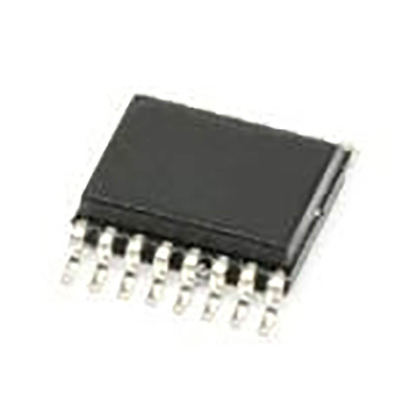
16-lead TSSOP and 16-lead, 4 mm × 4 mm LFCSP
APPLICATIONS
Communication systems Medical systems Audio signal routing Video signal routing Automatic test equipment Data acquisition systems Battery-powered systems Sample-and-hold systems Relay replacements
GENERAL DESCRIPTION
The ADG1611/ADG1612/ADG1613 contain four independent single-pole/single-throw (SPST) switches. The ADG1611 and ADG1612 differ only in that the digital control logic is inverted.The ADG1611 switches are turned on with Logic 0 on the appropriate control input, while Logic 1 is required for the ADG1612 switches. The ADG1613 has two switches with digital control logic similar to that of the ADG1611; the logic is inverted on the other two switches. Each switch conducts equally well in both directions when on and has an input signal range that extends to the supplies. In the off condition, signal levels up to the supplies are blocked.The ADG1613 exhibits break-before-make switching action for use in multiplexer applications. Inherent in the design is the low charge injection for minimum transients when switching the digital inputs.The ultralow on resistance of these switches make them ideal solutions for data acquisition and gain switching applications where low on resistance and distortion is critical. The on resistance profile is very flat over the full analog input range, ensuring excellent linearity and low distortion when switching audio signals.The CMOS construction ensures ultralow power dissipation, making them ideally suited for portable and battery-powered instruments.
PRODUCT HIGHLIGHTS:
1. 1.6 Ω maximum on resistance over temperature.
2. Minimum distortion: THD + N = 0.007%.
3. 3 V logic-compatible digital inputs: VINH = 2.0 V, VINL = 0.8 V.
4. No VL logic power supply required.
5. Ultralow power dissipation: <16 nW.
6. 16-lead TSSOP and 16-lead, 4 mm × 4 mm LFCSP


